Skip to content
James Cronin
Back to Handshake

Handshake build log

5 entries, newest first

  1. Five for five, after one blank header

    The cards arrived and all five work. Tap one with an iPhone and this page opens, from roughly 4 to 5 cm away. Getting there took a run of misleading errors and one section of the datasheet.

    First tap: nothing

    Every app could see the card and none could write to it. NFC Tools said the tag wasn't supported. NXP's TagWriter rejected the link as invalid. Another app said the tag "moved too soon", and another said it wasn't NDEF compliant.

    The hardware looked fine straight away. NXP's TagInfo identified a genuine NTAG I2C plus 1k, 50 pF, and passed its originality signature check. So the coil was powering the chip and the assembly was good.

    The wrong theory

    Reads worked and writes failed, and writing takes more power than reading, so I suspected the coil was only just getting enough energy. I had a plan to measure the tuning and fit the capacitor. It was a reasonable story and it was wrong.

    What ended it was reading the tag's actual state: a scan export said isNdefCapable: true, isNdefFormatted: false, ndefMaxSize: 0. It was like a new USB drive that the computer can see but can't save a file to.

    The answer was in the datasheet

    Section 8.3.10 says it plainly. The Capability Container on page 3 ships as all zeros on purpose, so the memory can be split however the application needs, and the user has to initialise it. NFC stickers sold ready to use have typically had this done already. A bare chip on your own board hasn't.

    Over NFC those header bits are one-way: a bit set to 1 can't be cleared. Undoing a typo would have meant going through the I2C test pads, so these writes needed care. It takes two raw writes, the empty NDEF message first and the header last:

    A2 04 03 00 FE 00    page 4: empty NDEF message
    A2 03 E1 10 6D 00    page 3: NDEF, version 1.0, 872 bytes, open access
    

    One more wall

    The plan was a small iPhone app to send those commands. It compiled, then failed at signing: Apple only allows NFC tag reading on the paid developer program. NFC Tools can send raw commands itself, so the app turned out not to be needed. Each write came back 0A, the chip's acknowledge. After that, a normal app could write the link.

    Results

    • All five cards work. Each opens this page from an iPhone, no app needed.
    • Read range is roughly 4 to 5 cm, by hand. The target was 1 to 3 cm.
    • The tuning capacitor isn't needed so far. The pads stayed empty.

    What I didn't do

    • The resonance is unmeasured. I never put a card on a NanoVNA, so the 14.1 MHz prediction is untested. The read range says it's close enough; it doesn't say how close.
    • There's no tap counter. All five cards open this same page, and the per-card links from the original plan aren't built.
    • The cards aren't password-protected yet, so their links can still be rewritten.

    What I'd keep

    • Read the actual state before building a theory.
    • A blank part may need setting up before it behaves like the finished product.
    • Read the delivery-state section of a datasheet before the parts arrive.

    Five cards, first revision, no rework. That's this project finished.
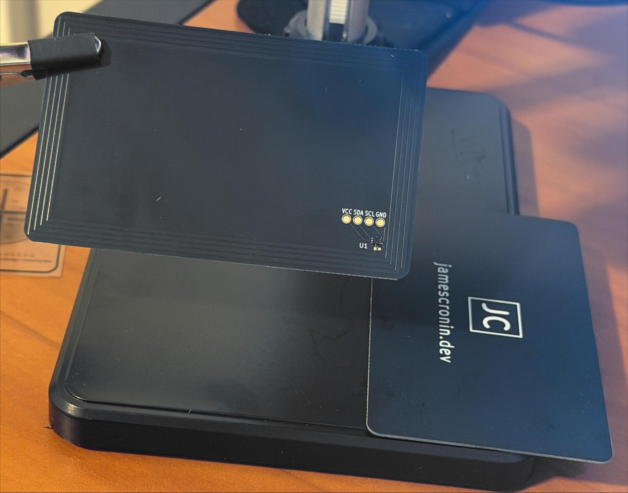
    • Rev A in hand. Parts side above, with the four coil turns under the mask, the labelled gold pads and the chip. Logo side below. Photo cropped and colour-corrected to reduce a blue reflection.
  2. Rev A ordered

    Five cards are on order from JLCPCB, assembled. While they ship, the site gets the page each card will open.

    The order is five boards at 0.8 mm with a black mask and ENIG, with the chip placed and soldered by JLCPCB. They also remove the edge rails the assembly line needs to hold a board this narrow, so the cards arrive with clean edges. JLCPCB's engineers check the chip's rotation against the placement file before they solder.

    Most of the cost of a first run like this is fixed: assembly setup, shipping and import duties. Spread across a larger batch, the cost per card falls sharply.

    While they ship

    Each card will open its own link, like jamescronin.dev/h/01. That page doesn't exist yet, so it's next: a route that counts taps per card and greets the visitor. Then, when the boards arrive, every card gets measured on a NanoVNA against the 14.1 MHz prediction and programmed from a phone.

  3. Rev A layout, ready to order

    The card is laid out. One chip, a four-turn coil, two vias, and a design-rules check with nothing on it. The order files for JLCPCB are generated.

    The coil

    The antenna is a footprint generated by a short Python script rather than drawn by hand. It walks the spiral around the card, checks the gap between turns and the distance to the board edge, and refuses to write a footprint that breaks either rule. That check moved the coil 0.2 mm further in than the plan: the card's corners are rounded and the coil's are square, so at a 1 mm inset the coil's corners came within 0.26 mm of the edge, under the 0.3 mm a board house needs. Inductance moved from 2.56 to 2.54 µH, and the resonance stayed at 14.1 MHz.

    Placing the chip

    The chip is rotated so its two antenna pins face the two ends of the coil, and the last turn ends directly under one of them, so that connection is a single straight 1.5 mm track. The other end has to cross the turns to reach the chip, which it does once: a short 45° bridge on the back layer with a via at each end. My first pass at routing needed six vias, because the chip faced the wrong way. Turning it first got that down to two.

    Room to tune

    Under the chip are two empty pads for a 0402 capacitor across the antenna. The bare card should resonate around 14.1 MHz. The capacitor's value comes from measuring each card: one at 14.1 MHz needs about 4 pF to land on 13.56 MHz, one at 14.5 MHz about 7 pF. Leaving the pads empty costs nothing on the order.

    Programming pads

    VCC, SDA, SCL and GND come out to four 1.5 mm pads on a 2.54 mm grid, labelled by function, so a pogo-pin jig can write the tag over I2C if a phone can't. They're ordered to match the chip's pins, so none of the four tracks cross.

    Checks

    Design-rules check: no violations, no unconnected items, and the board matches the schematic exactly. The order files for JLCPCB (Gerbers, drill, parts list and placement) are generated; only the chip needs placing.

    Next

    Order a small first batch, then measure every card on a NanoVNA.

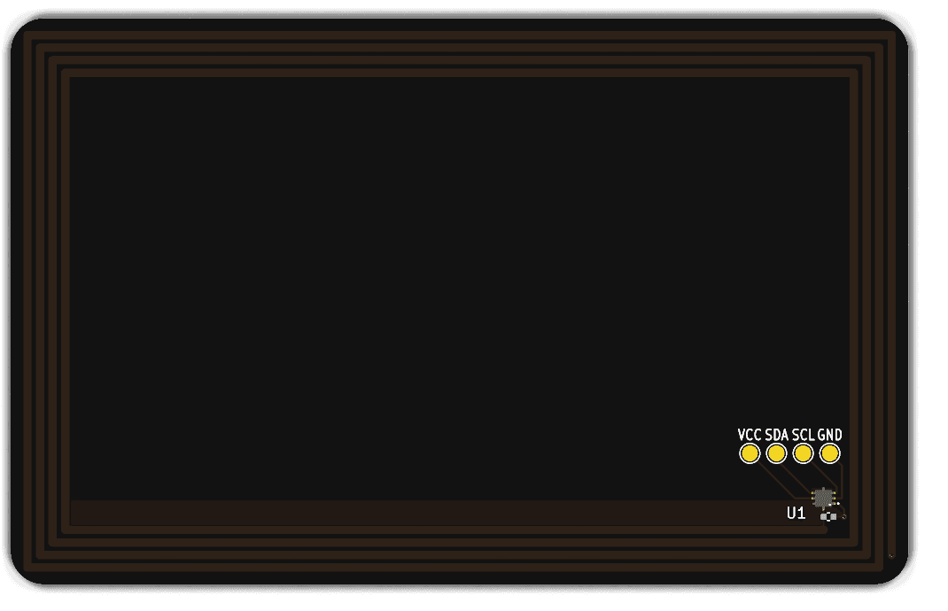
    • Rev A, parts side: the four-turn antenna around the card edge, the NFC chip and its programming pads in the corner. Rendered in KiCad, black mask, ENIG.
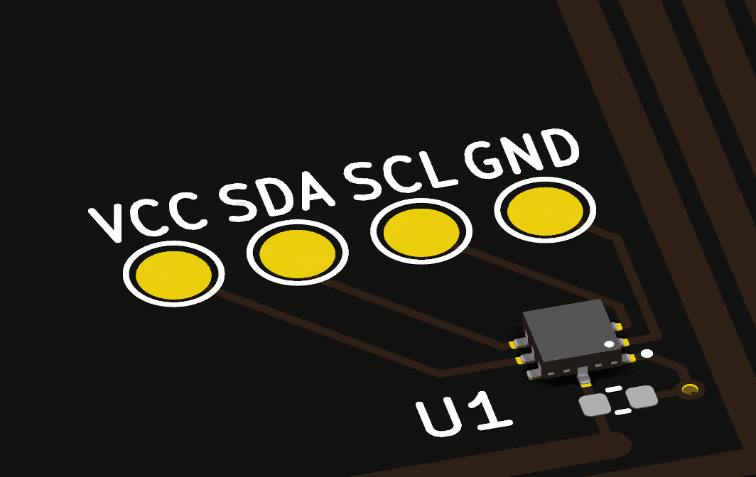
    • Close-up: the chip rotated so both antenna pins face the coil ends, the empty tuning-capacitor pads below it, and the via where the antenna bridge drops to the back.
    • Rev A, back: the JC mark and jamescronin.dev in silkscreen.
  4. Schematic done, and the simulation agrees with the maths

    The schematic passes the electrical rules check with every unused pin given a deliberate job. Then I simulated the antenna as a resonant circuit, and the peak landed at 14.1 MHz, exactly where the hand calculation put it.

    The schematic

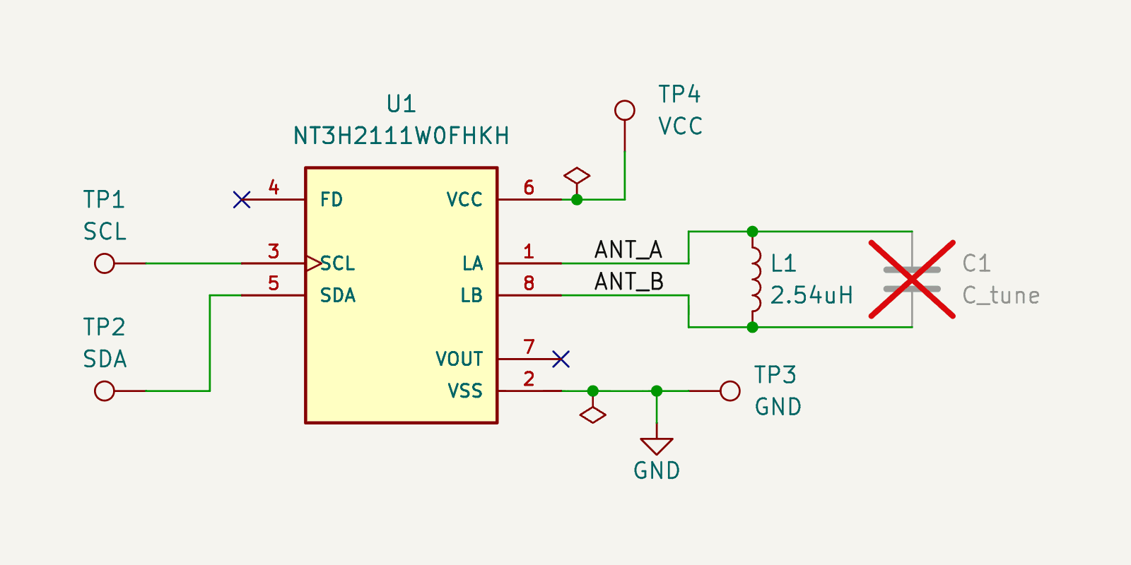
    The circuit is small, so the work is in deciding what every pin does. Only the two antenna pins, LA and LB, work during a tap, with the coil across them. Of the rest:

    • FD and VOUT are no-connects. FD signals a host microcontroller that a field is present, and VOUT supplies one. There is no host on the card.
    • SCL, SDA, VCC and GND go to 1.5 mm test pads. On a tap they do nothing, but they let a pogo-pin jig write the tag over I2C if a phone app can't format it. That's free insurance against a known risk with this chip.
    • VCC and GND carry power flags. The checker expects every power pin to be driven by something on the board. Here the supply comes from the jig, off the board, so the flags record that this is deliberate.

    The electrical rules check is clean. The coil is the only part still without a footprint; it gets drawn as copper next.

    The simulation

    Electrically the card is three things in parallel across LA and LB: the coil (L = 2.56 µH), the chip's input capacitance (C = 50 pF from the datasheet), and the power the chip draws, modelled as a resistor (R = 5 kΩ, an estimate, since NXP doesn't publish it).

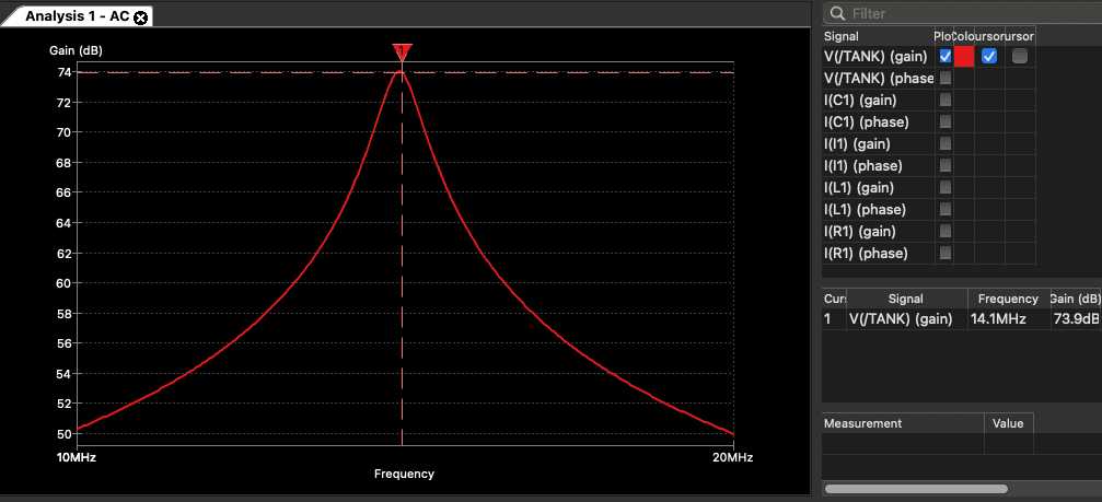
    I drove that circuit with a 1 A AC test current in KiCad's built-in ngspice and swept 10 to 20 MHz. With 1 A in, the voltage is the impedance. The peak is at 14.1 MHz, against 14.07 MHz by hand. Its height, 73.9 dB, is about 5,000 V for 1 A, which is 5 kΩ: at resonance the coil and capacitor cancel and only the resistor is left, as they should.

    The −3 dB points sit at 13.7 and 14.4 MHz, a Q of about 20. The phone always transmits at 13.56 MHz, just below that window, where this model gives about half the voltage of the peak. That fits the plan: the bare card resonates slightly high, because board capacitance and the phone's own coil both pull the resonance down, and about 4 pF of tuning capacitor lands it on 13.56 MHz if measurement says it needs to. The resistor value is the biggest unknown; a heavier load lowers Q and widens the window, which is why every first card gets measured on a NanoVNA.

    Next

    Draw the four-turn coil as a footprint, then start the card layout.

    • Rev A schematic: the NT3H2111 with the antenna coil L1 across LA and LB, the optional tuning capacitor C1 (marked not fitted), test pads TP1 to TP4 on the I2C, VCC and GND pins, and no-connects on FD and VOUT.
    • AC sweep from 10 to 20 MHz in KiCad's ngspice simulator: a single resonant peak at 14.1 MHz, 73.9 dB.
  5. Architecture, and why the antenna has four turns

    Handshake is a business card that is also an NFC tag. The whole design comes down to one chip JLCPCB can place and one coil that has to resonate at 13.56 MHz. Both are now pinned down, and the schematic is started.

    The card is a 0.8 mm board at bank-card size with no battery. A phone's NFC field powers it for the length of a tap, and the chip answers with a link unique to that card. The architecture is written up as HSK-HW-001.

    The chip

    The obvious NFC tags, NXP's NTAG 213/215/216, are sold as wafer or inlay, not in a package an assembly line can place. The NTAG 424 DNA would sign every tap, but had no stock. ST's ST25DV is ISO 15693, which phones read at a shorter range. That leaves the NXP NT3H2111: an NFC Forum Type 2 tag in a 1.6 × 1.6 mm XQFN-8, in stock at JLCPCB. It has an I2C port meant for a host microcontroller. There is no host here, so only its two antenna pins work during a tap.

    The antenna

    The coil and the chip's own input capacitance form the resonant circuit. NXP gives that capacitance as 44 to 56 pF, 50 pF typical, so landing on 13.56 MHz needs about 2.76 µH.

    Inductance in a flat spiral rises roughly with the number of turns to the power 1.8, so each turn matters a lot. The first plan said five or six turns. Running NXP's coil formula (AN11276) for a coil 1 mm inside the card edge, five turns give 3.74 µH and resonate near 11.7 MHz, far too low to read well. Four turns of 0.8 mm track give 2.56 µH and a bare resonance of about 14.1 MHz.

    Landing slightly high is deliberate. Board capacitance pulls the resonance down, and the optional tuning capacitor can only lower it further. A card that starts below 13.56 MHz can't be fixed without cutting copper. Every Rev A card will be measured on a NanoVNA.

    First steps in KiCad

    The chip's symbol and footprint came from SnapEDA. Before trusting the footprint I checked it against NXP's package drawing (SOT902-3): 0.5 mm pitch, pin 1 in the right place, and no centre pad, because NXP marks that metal area "not for soldering". The two single pins at the top and bottom have pads slightly narrower than the chip's terminals, which I'll widen. The chip and the antenna are placed and connected.

    Next

    Decide what each unused pin does (programming pads or no-connect), draw the coil as a footprint, then lay out the card.