Skip to content
James Cronin
Back to Jot

Jot build log

16 entries, newest first

  1. Order files and a first quote

    Gerbers, drill files and assembly files are done, and a first JLCPCB quote came back at about $200 for five assembled boards. The order goes in once the radio modules land in stock and Raytac has checked the antenna area.

    With the layout finished, the next job was turning it into files a factory can build from, and finding out what it costs.

    The order files

    Four sets of files go to JLCPCB:

    • Gerbers. One file per layer: four copper layers, the solder mask and silkscreen on each side, the solder paste and the board outline.
    • Drill files. 182 plated holes (vias, the USB socket's shell and the wire pads) and 10 unplated ones (mounting holes, locating pegs for the USB socket and the button, and the two microphone sound holes). The counts match the board exactly.
    • Parts list. 34 lines, 65 parts, each matched to a JLCPCB or LCSC part number.
    • Placement file. The centre and rotation of every part.

    All of it is exported to JLCPCB's published KiCad settings. The board is 37 × 62.6 mm overall once the USB tab is counted, and JLCPCB prices by the overall size.

    What the first upload turned up

    The parts list matched on the first upload, with three exceptions:

    • The accelerometer is assembly-restricted. It's a 2 × 2 mm LGA with its joints underneath, and JLCPCB only places it on their Standard assembly line, which X-rays the joints. The order moves from Economic to Standard rather than changing a part on a finished board.
    • The microphone needed buying in. It's in stock at LCSC but wasn't in JLCPCB's assembly stock yet, so it comes in through the parts library.
    • The radio modules aren't there yet. The six Raytac modules were pre-ordered on 8 October and are due around 22 October.

    The quote

    About $200 all in for five assembled boards, on top of $110 already spent on the six radio modules. That is five complete boards, each with every part fitted except the battery, motor and NFC antenna, which go in by hand.

    Before the order goes in

    Raytac offers a free review of the antenna area on boards using their modules, and that request is out now. With their answer and the modules in stock, the order goes in. The batteries, motors and NFC antennas are ordered separately in the meantime, along with a debug probe for the first firmware flash.
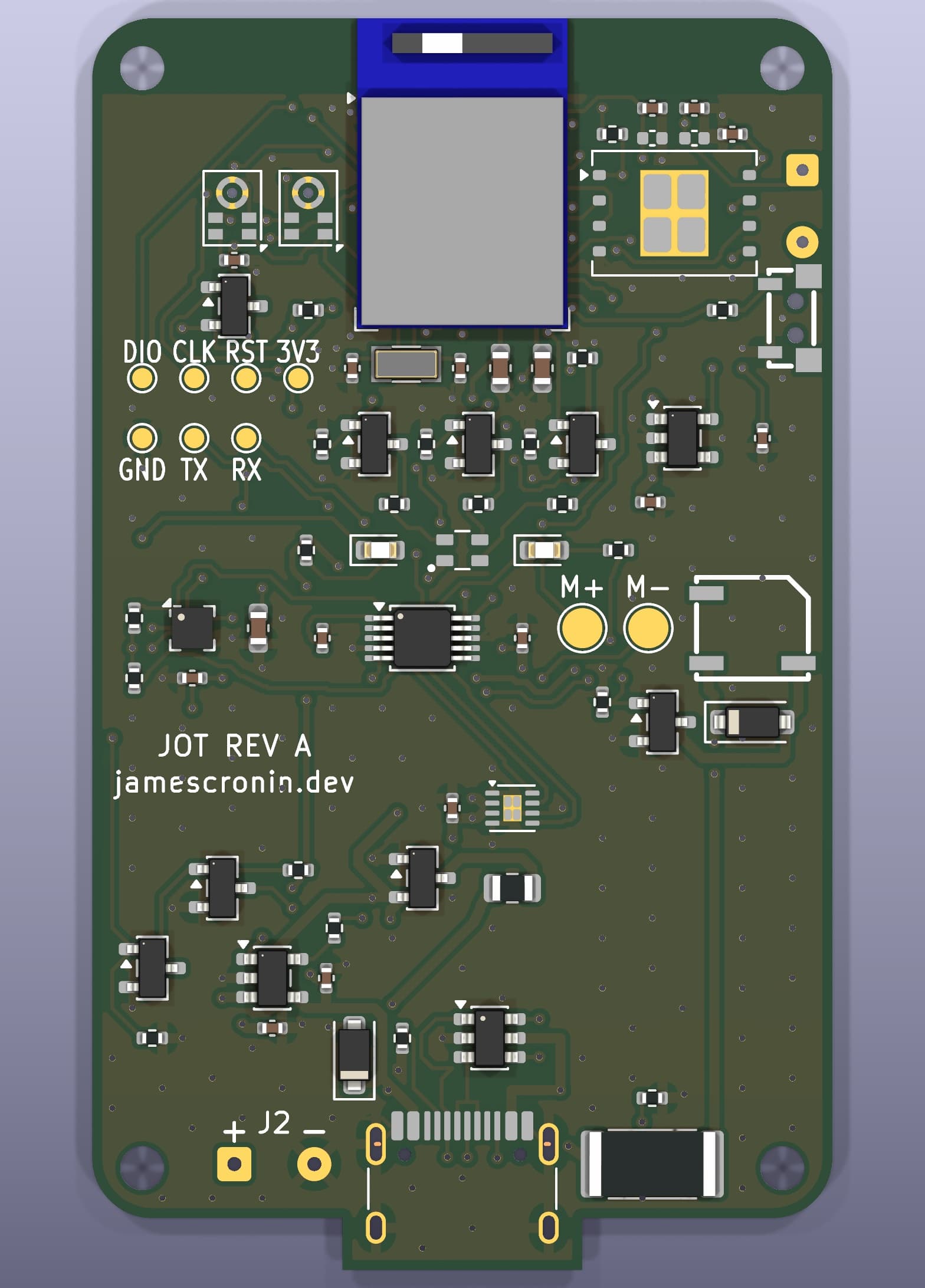
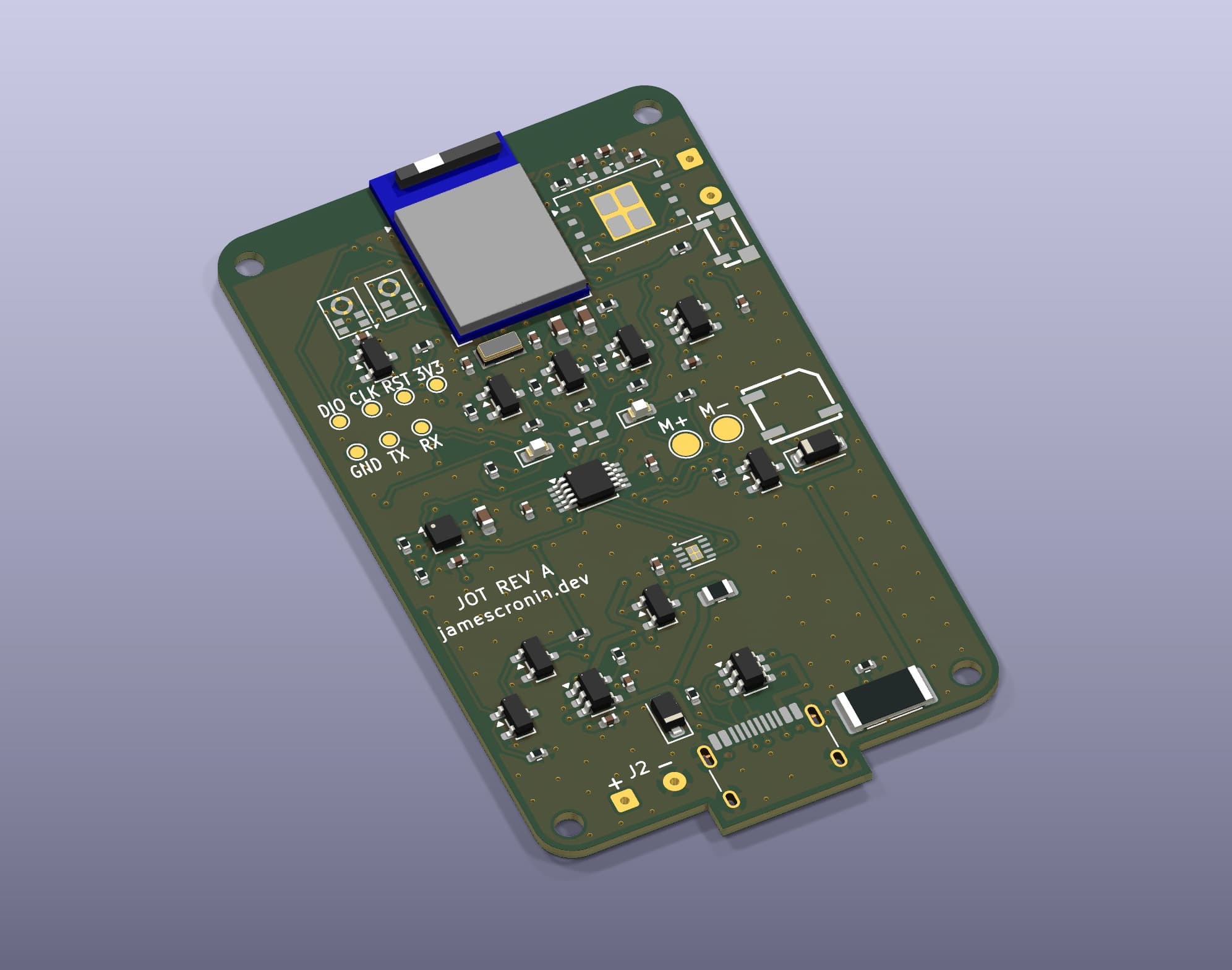
    • Top view render of the Jot Rev A board, the version going to fabrication.
  2. Layout finished

    Every connection is routed and the board has been through a full layout review. The fixes changed the battery connection, the LED pin order and how the module's inner pins get out. The design-rule check is clean and the board matches the schematic.

    The last connections were the memory, the microphones, the sensors and the simple lines to the button, buzzer, LEDs and test pads. With everything routed, the board went through a full layout review before ordering. The review looked for anything that would cost a respin. Six things came out of it.

    The battery connector didn't fit

    The JST battery header stands 5.5 mm off the board. The board's top face sits 8.1 mm above the back of the case, so the header would end 13.6 mm up, 0.8 mm outside a 12.8 mm case. Soldered leads take no height at all, so J2 became two solder holes, marked + and − on the silkscreen. The battery leads go up through them from underneath, and the reverse-battery switch is still on the board in case one goes on backwards.

    No drills in pads

    Some of the radio module's inner pins had been escaped with a via drilled straight through the pad. On a 4-layer board without filled vias, solder can drain down an open via and starve the joint. Each one now sits beside its pad, with the hole at least 0.1 mm clear of the pad's solder opening and covered by solder mask.

    Matching the LED pins to the board

    Three module pins drive the red, green and blue switches, but they ran blue, red, green along the module edge while the switches sit red, green, blue below it. The blue line had to loop over the other two to get out, and that loop was what forced the vias into the pads. All three are plain GPIOs driving transistor gates, so the fix was in the schematic: P1.08 is now red, P0.11 green and P0.12 blue. Each line now drops straight down to its switch.

    Keeping the crystal quiet

    Nordic's guidance is to keep other signals away from the 32.768 kHz crystal. There's now no top-layer track or via of any other net beside it. Four signals still pass underneath on the bottom layer, with the solid ground plane on layer 2 between them and the crystal.

    Smaller fixes

    • Buzzer resistor moved. R19 dissipates real power if the buzzer ever sticks on, so it moved off the battery.
    • Short ground returns. The module's ground pads and the decoupling capacitors got their own ground vias.
    • Clean USB return path. A 5 V branch came off the power layer so the USB pair runs over unbroken copper.
    • Readable silkscreen. The test pad and motor labels went up to 1.0 mm text so they survive the board house's minimums.
    • Case. A 0.4 mm pocket inside the front shell clears the side switch, and the alignment lip went from 0.6 to 0.8 mm after the printer flagged it as a thin wall.

    The design-rule check is clean, the board matches the schematic, and the schematic, renders and copper layers are now on the Jot page.

    Next

    Raytac offers a free layout check of the antenna area, so that goes first. Then Gerbers and assembly files to JLCPCB for five boards, two of them assembled.

    • Render of the finished Jot Rev A board: the radio module at the top edge, test pads on the left, USB-C on a tab at the bottom.
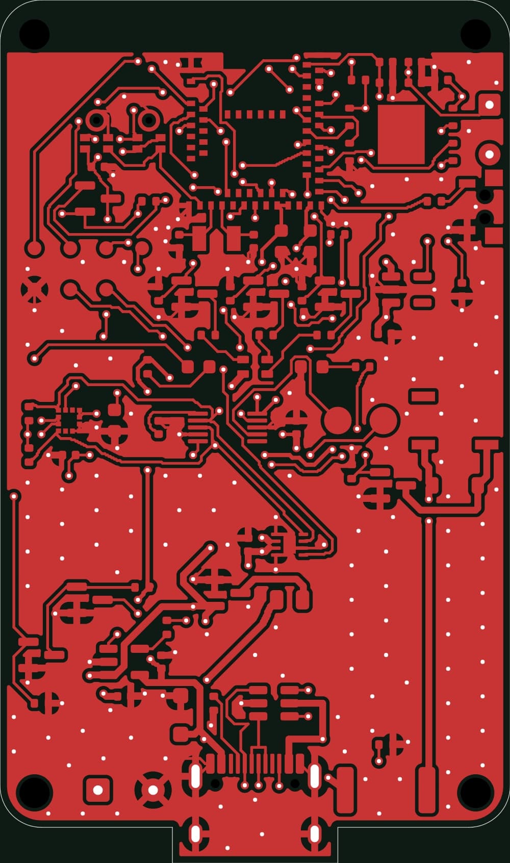
    • The top copper layer of the Jot Rev A board on a dark background.
  3. Routing the hard parts first

    USB, power and the radio module's tightest pins are routed, and a layout review moved three parts before they got locked in. About a third of the connections are left, mostly the easy ones.

    The order matters more than any single track. Anything routed early takes space from everything after it, so the plan was to start with the signals that have the least freedom and let power and the simple lines fit around them.

    The USB corner

    The bottom of the board is the densest spot on it: the USB-C socket, its ESD chip and two resistors in about 10 × 8 mm, with five nets fighting for the same gap. USB-C also has every data pin twice, interleaved D−, D+, D−, D+, so the two pairs can't both be joined on the top layer. The D− pins join underneath through two vias under the socket body, the D+ pins bridge on top, and the CC lines drop to the bottom layer too. My first 5 V route closed a loop around the ESD chip with four signals inside it, so that came out and went back in a different shape.

    From there the USB pair runs as a pair on the bottom layer, about 0.35 mm apart, up to the module. At full-speed USB the 4 mm length difference doesn't matter.

    Planes

    Layer 3 is now two copper areas: 3.3 V across the top of the board where the module and memory are, and battery voltage everywhere else. Every power pad drops straight into its area through a via, which cleared about thirty connections without a single long track. The shape of the 3.3 V area leaves a battery-voltage strip under the USB pair, so the pair never crosses the split.

    Reviewing before it sets

    With the hard parts in, I ran a layout review. Nothing was wrong enough to stop a board, but three placements were worth fixing while it was still cheap. The charger's input capacitor had ended up 12 mm from the charger, the USB surge diode 8 mm from the socket, and the clear area beside the antenna was only as wide as the module. Raytac's guidance is to keep it as wide as the board allows. The capacitor and diode moved next to the parts they protect, the antenna got more clearance along the top edge, and the planes now keep a tighter 0.25 mm gap around vias so they stay closer to solid copper.

    The module's inner pins

    The Raytac module has two staggered rows of pads down each side, and between two outer pads there's only 0.4 mm. An inner pin can't squeeze out through that, so it goes inward instead, under the module to a via, and leaves on the bottom layer. That's how the NFC lines got out. The crystal went straight down from its pins, a few millimetres each side and mirrored.

    The RGB LED got turned 180° in place, still centred under its dot, so its three cathodes line up with their resistors instead of crossing.

    Next

    About 65 connections left: the memory chip, the microphones, the sensors and the simpler lines to the button, buzzer and test pads. Then a final review before the order.

  4. Laying out the board

    Rev A has its outline, every part placed and its ground plane in. Fitting the board to the case moved the USB socket and changed how NFC works.

    The case came first so it could set the board: 37 × 60 mm, four layers, 1.0 mm thick, with four M2 holes where the case's screw posts land and rounded corners that clear the lip lining up the two halves.

    Fitting it to the case

    Every part that meets the outside world gets checked against the case before it goes down. The USB-C socket failed that check. With the board edge where the case model put it, the socket's mouth sat 3.5 mm behind the outside of the case, and a plug has only about 6.6 mm of metal in front of its grip, so it would never have seated. The board now has a small tab under the socket that carries it forward into the wall opening, 0.9 mm from the surface, and the case has a matching gap in its lip.

    The side switch only travels 0.15 mm, so the button's inner flange is now thick enough to sit 0.08 mm off its plunger. The case also picked up a slot for the buzzer and moved its mic opening over the microphone.

    Placement

    The parts the case fixes went down first: the USB socket, the button, the three lights under the front dots and the radio module. The top end is the only part of the board without the battery behind it, so the module sits there with its antenna on the edge. Everything else followed the module's pinout. The memory sits beside its pins on the module's right, the microphone top left over the open space under the board, and the charger and battery input at the bottom next to their connectors.

    NFC moves off the board

    The plan was an NFC coil drawn in copper. Placement showed it can't work here. A coil needs about 20 × 20 mm with no copper on any layer inside it, and the only area without the battery behind it belongs to the Bluetooth antenna. NFC now uses a ferrite-backed flex antenna, 0.27 mm thick, in a pocket inside the back shell, the same arrangement phones use, so you tap the back of Jot on the phone. The tuning capacitors went from 180 pF to 82 pF to suit its 3.1 µH, with two empty pads beside them for fine-tuning on the first board.

    Routing

    Layer 2 is one unbroken ground plane, and every ground pad on top has a via beside it down to that plane: 43 of them. Power has its own net class at 0.5 mm, and USB power now runs from the socket through the surge diode to the charger.

    The USB corner is the tightest spot on the board: the socket, its protection chip and two resistors in about 10 × 8 mm. The first 5 V route closed a loop around the protection chip with four signals inside it, so one side of it came out again. From here the order is the delicate signals first, the USB data pair and the crystal, with power fitted around them.

    Next

    Finish the USB corner, bring the module's pins out, then the rest of the power and signals, and a full layout review before ordering.

  5. A case for five

    The first case model: 68 × 42 × 12.8 mm, two halves held by four screws that also clamp the board. A flatter, bigger battery took it from 16 mm thick to under 13.

    With the schematic done, the case comes next, because its shape sets the board outline for layout. I started from the concept render: a dark slab, about 1.6 times as tall as it is wide, with big rounded corners, three dots in the middle, the logo near the bottom and an orange button on the right edge.

    Thickness

    The first version came out 16 mm thick. Half of that was the battery: the Adafruit cell I'd planned on is 7.8 mm deep. Adafruit also sells a 5 mm thick cell that actually holds more, 500 mAh instead of 400, and with 1.2 mm walls instead of 1.5 the case is now 12.8 mm. The last millimetre or so is the USB-C socket, which can shrink in a later revision.

    Holding it together

    Four M2 screws go in from the back, through posts that the board sits on, through the board itself, and into bosses inside the front half. Tightening them clamps the board and pulls the two halves together, so there's nothing on the front. A thin lip on the back half slides inside the front half to line them up. Small ribs stop the battery sliding around underneath the board.

    Details

    The button has three grooves so a thumb finds it without looking, and a flange on the inside so it can't fall out. The dot over the j is a separate orange piece. The mic hole sits below the board, because the microphone hears through a hole in the PCB rather than from the top.

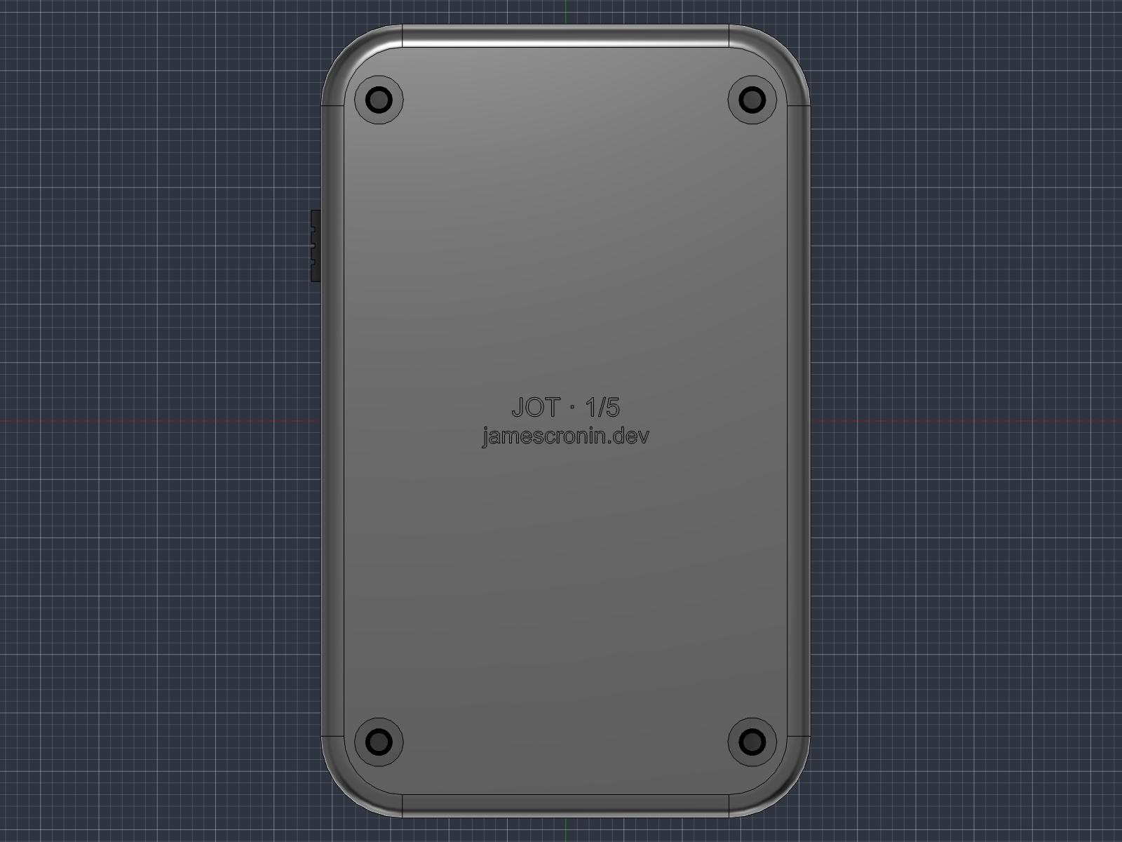
    There will be five of these, so the back of each one is numbered, 1/5 to 5/5, above the site address.

    Still to do

    Light pipes behind the three dots, the sound channel from the case to the mic, and how the button presses the switch. Those depend on where parts land on the board, which is the next job.

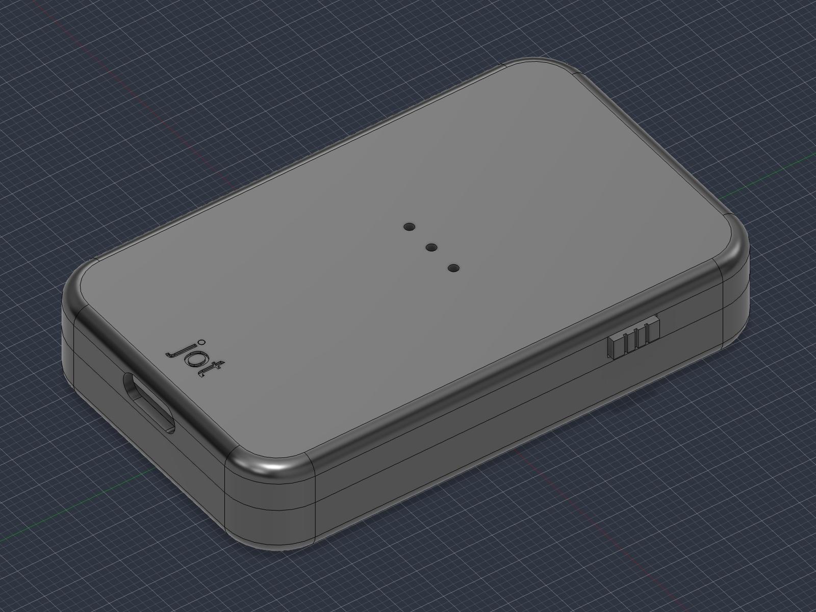
    • Jot case v1 model: rounded slab with three front dots, the jot logo, a grooved side button and the USB-C opening.
    • The back of case v1: four recessed screws and the engraving JOT · 1/5, jamescronin.dev.
  6. Finishing the schematic

    Before layout I went through the schematic one last time, asking what happens when each part fails rather than whether it works. That added a fuse, reverse-battery protection, a surge diode on USB and a way to stop charging when it's too hot or cold, and swapped the flash for one an eighth of the price.

    Before starting the PCB layout I did one more pass over the schematic, this time asking what happens when each part goes wrong rather than just whether it works. Some choices held up, like running the LEDs and buzzer from the battery rather than 3.3 V (so the LEDs still light when the battery is low, and the buzzer's current spikes stay off the microphone supply). Others didn't, and I spent tonight fixing them.

    The battery

    This was the biggest one. The pack has its own protection board, but it only cuts out somewhere between 2 and 5 amps. A fault drawing less than that, say a shorted capacitor or a solder bridge, would just get hot. There's now a resettable fuse at the battery connector that trips at 1 A. I checked its datasheet derating too: it holds 0.5 A at room temperature but only 0.33 A at 60 °C, which is still above the worst load I could add up (about 245 mA with the radio, flash, buzzer and motor all running at once). Next to it is a P-channel MOSFET, so a battery plugged in backwards can't power the board.

    USB and charging

    The charger's datasheet says USB needs overvoltage protection because plugging in a cable makes the voltage ring, so there's a 5 V TVS diode right at the connector now.

    The cell can only be charged between 0 and 45 °C, and the charger can't measure temperature. Two small transistors now let the firmware switch charging off. They default to charging when the processor is off, because a flat battery has to be able to recover. The firmware uses board temperature rather than the cell's, so it's a halfway measure; a charger with a proper temperature input is on the Rev B list.

    Smaller stuff

    The I2C pull-ups went from 4.7 kΩ to 2.2 kΩ: the fuel gauge alone can add 60 pF to the bus, which left almost no margin. I'd assumed 4.7 kΩ was fine without checking. The buzzer resistor is now a 1 W part, because a firmware bug that left the buzzer on would have put half a watt into a quarter-watt resistor. The button has a 1 kΩ resistor in series for static protection, since these are going to be handed to people.

    A cheaper flash chip

    I'd picked a 128 MB chip at $36 each. Jot only keeps recordings until the next sync, and 32 MB is about an hour of audio, so it's now a 32 MB chip in the same package for $4.34. That's about $160 off the first five boards.

    Still open

    Not everything is solved. A backwards battery with USB plugged in at the same time can still push a small current the wrong way, and a big enough USB surge could get past the diode. Those are written down in the architecture document with what Rev B does about them. The radio module and haptic driver are on pre-order, the BOM uploads cleanly to JLCPCB, and the schematic is done. Layout starts once I've measured the case.

  7. Every part has a footprint

    The schematic says what connects to what. Footprints say what copper each real part sits on. All 68 parts that get bought and soldered now have one, each checked against its datasheet drawing. The 69th, the NFC coil, is drawn in copper later.

    A footprint is the pattern of copper pads a part gets soldered to. Get one wrong and nothing complains until the boards arrive: a chip rotated, a pin landing on nothing, an LED backwards. So this stage was mostly reading package drawings.

    How each part got its footprint

    • KiCad's own library for most of the board. The trick is reading the name: WSON-8-1EP_8x6mm_P1.27mm_EP3.4x4.3mm is the flash's package, body size, pitch and exposed pad, and every number has to match the datasheet's table.
    • A download, checked. The fuel gauge's datasheet doesn't contain its drawing; the package code points to a separate outline document. A SnapEDA footprint confirmed which of eight look-alike footprints was right: they differ only in the exposed pad.
    • JLCPCB's own footprints for the side switch and the buzzer, pulled from their library with a tool called easyeda2kicad. The switch's locating posts came through as plated holes with no copper ring, so they became plain drilled holes.
    • Built from the datasheet for the RGB LED, from its recommended pad layout. Lesson: the drawing wasn't to scale, so only the labelled numbers count.

    Two traps worth remembering

    • A pin diagram that looks mirrored. The accelerometer's datasheet shows pin 1 top-right, but the footprint has it top-left. The package drawing explains it: that diagram is a view from underneath.
    • Battery polarity. JST battery plugs have no universal standard. Jot matches the convention Adafruit and SparkFun share, and a multimeter check on the real battery will confirm it.

    A script now checks that every pin on every symbol has a matching pad. It found none missing. The only part without a footprint is the NFC coil, which is drawn in copper once the board outline exists.

    Next

    PCB layout: the board outline, then placing the parts where the case needs them.

  8. A charger too small to assemble

    Before assigning a single footprint, I checked that JLCPCB could actually build and assemble the board. One part couldn't be placed, so it's gone.

    I don't want bare boards for Rev A. Hand-soldering dozens of 0402 parts isn't a good use of a first prototype, so the plan is for JLCPCB to assemble it. Before starting footprints, I checked the whole design against their assembly capabilities.

    Almost everything fits: four layers, 0402 passives, the 0.5 mm-pitch fuel gauge, accelerometer and mic. The nRF52840 module isn't stocked by their parts library, but they accept consigned parts, so I'll post them a few.

    The problem

    The charger, a TI BQ25101, comes in a ball-grid package with 0.4 mm between its six solder balls. JLCPCB's economy assembly line only places ball-grid parts down to 0.5 mm. Their standard line can go finer, but only on panels at least 70 × 70 mm, which would mean a panel of eight to twelve Jots at a much higher cost. And if that chip ever needed replacing on a first board, it couldn't be done by hand.

    The fix

    It's now a Microchip MCP73831, one of the most widely used LiPo chargers, in a SOT-23-5 package anyone can solder. The charge current stays at about 200 mA, set by one resistor (1000 V ÷ 5.1 kΩ), and the charge LED works the same way. It has no battery-temperature input, but the pack has no thermistor, so nothing is lost.

    I now check that every part can be assembled before I place it. Found now, this cost an evening. Found after layout, it would have cost a board revision.

    Next

    Footprints for every part, with each one checked against its datasheet and the exact LCSC part JLCPCB will place.

  9. Schematic complete, and a second pair of eyes

    All nine Rev A sheets are drawn in KiCad. Then two independent reviews went over every pin, net and datasheet limit, and four things changed before any copper exists.

    The last five sheets went in today: the accelerometer and haptic driver, the button, RGB LED and buzzer, the debug pads and the NFC antenna. That makes nine sheets and 70 parts, with every net checked against the pin list as it was drawn.

    A schematic that passes its own checks can still be wrong, so it then got a full review from two reviewers working separately, each checking connections against the datasheets before comparing notes. Both found that every custom symbol's pin numbers match their datasheets. Between them they also found the following.

    What changed

    • The flash could start up confused. Its chip-select floated while the nRF52840 powered up, and Winbond asks for it to follow the supply. A 100 kΩ pull-up now holds it off.
    • The buzzer was over its rating. It's rated to 4 V and runs from a battery that reaches 4.2 V, and nothing limited the current if its switch were ever left on. A 10 Ω resistor now sits in series.
    • The battery outlives the flash. The pack's protection cuts off at 2.5 V, but the flash needs 2.7 V and should be read near the voltage it was written at. The plan is for the fuel gauge to shut Jot down well before that.
    • The I²C bus needs to slow down. The fuel gauge's pins add enough capacitance that 400 kHz has no margin. The plan is to run it at 100 kHz, which is plenty for these chips.

    A few more are firmware rules rather than parts. The main one: the mic clock has to stop before the mic rail switches off, so the recording light can't glow with the mic off.

    Next

    Footprints for every part, then PCB layout. The schematic files will be published once the board is laid out too.

  10. Schematic, half way

    Four of the eight Rev A sheets are drawn in KiCad, with power, the nRF52840, flash and audio all wired. Checking each step against the pin list caught four mistakes before they reached copper.

    I'm drawing it one block at a time in KiCad and checking each step against the pin list before moving on. Every check exports the netlist and runs KiCad's electrical rules check.

    What's drawn

    • Power. USB-C with ESD protection, the BQ25101 charger and its charge LED, the battery connector, the TPS7A0233 3.3 V regulator and the MAX17048 fuel gauge.
    • MCU. The nRF52840 module, its supply caps from Raytac's reference circuit, the 32.768 kHz crystal, and a labelled net for every pin it uses. The 22 spare pins are marked unused on purpose.
    • Storage. The 128 MB flash on six QSPI lines. Its symbol is drawn from the Winbond datasheet.
    • Audio. The microphone, the footprint for a second one, and the switch that powers both. The Rec LED sits on that same switched rail, so the mic can't be on with the light off.

    What the checks caught

    • 5 V on the flash. Its supply was wired to USB power instead of the 3.3 V rail. It's rated to about 3.6 V, so it would have died the first time USB went in.
    • Two data lines swapped. IO0 and IO2 between the flash and the MCU were crossed. In quad mode every byte would have come back scrambled.
    • The crystal on the wrong pins. It was on the flash chip-select and the reset pin rather than the two pins with the oscillator behind them.
    • Two parts called U2. The flash and the mic had the same reference, which would have mixed them up at assembly.

    All four were small slips, which is why each step gets checked.

    Next

    Sensors (the accelerometer and haptic driver), the button, LEDs and buzzer, the debug pads and the NFC antenna. Then footprints and PCB layout. The schematic and board files will be published once both are finished.

  11. Making the app hold up

    The app worked for me. A full review, a list of my own change notes, and a pass through every screen turned up what would break for anyone else. Here's what changed.

    The iPhone app has run the whole loop for a week, but only for me: it needed my own Claude API key, and I knew how to avoid its rough edges. Before anyone else uses it, I went through the code and every screen looking for what would fail. The new screens are in the App tab.

    What could lose a recording

    • The mic could stay on. A phone call or pulling out AirPods stops the audio, and the old stop rules only ran when audio arrived. A wall-clock watchdog now ends every recording, and interruptions end it cleanly.
    • A failed transcription deleted the audio. Now the recording is kept as a voice note you can play back.
    • A store that wouldn't open ran on an empty, in-memory one. Everything captured would vanish on quit. The schema is now versioned with a migration plan, and a store that won't open stops the app with a clear message.

    What everyone else would need

    • No API key. Sorting goes through a route on this site that holds the key, with rate limits and a daily cap, and it never logs what was said.
    • Consent. A Smart sorting switch, off by default, says what's sent and to whom, with a privacy policy behind it.

    From my own change notes

    The app has a Develop tab where I record notes about Jot while using it. Two of them shaped this round:

    • The record orb covered the Delete button on the detail screen. The orb now stays off detail screens, and Delete lives in a menu with Undo.
    • I wanted to add a follow-up after a meeting. Any item can now have follow-ups, recorded hands-free from the item itself.

    Captures that couldn't be sorted are now sorted later automatically, reminders have Done and Snooze buttons, and there's a test suite, including a test that upgrades a real version-1 store file.

  12. Every part, checked against its datasheet

    The Rev A parts are chosen and the pin map is done. Before drawing a single wire, I read every datasheet and reference design, and five things changed. The BOM and pin list are now public.

    The architecture said what the board needs to do. This step was choosing the exact part for every job, assigning every signal to a pin on the module, and then checking all of it against the manufacturers' documents before the schematic, where mistakes are cheap to fix.

    What changed

    • A separate 3.3 V regulator. The nRF52840 can make 3.3 V itself, but its regulator starts at 1.8 V until firmware changes a setting, and it only supplies about 25 mA to other chips. The flash needs 2.7 V and draws up to 25 mA while writing. A TI TPS7A02 now powers the board, at 25 nA when idle.
    • Flash moved off the reset pin. The flash chip-select was on P0.18, which is also the chip's reset. It now uses the same pins as Nordic's development kit.
    • LEDs you can actually see. Green and blue LEDs need up to 3.6 V. Through 1 kΩ from a 3.3 V pin they'd get about 0.3 mA. Now 100 Ω.
    • The reference circuits win. 10 µF instead of 4.7 µF on the module's supplies, and a 2.2 Ω resistor on USB power, as Raytac and Nordic show.
    • A different microphone. The TDK T3902 replaced the Infineon IM69D130 because it's in stock for assembly. It gives up a few dB of signal-to-noise ratio (64 vs 69).

    Some values came from calculation: 18 pF crystal load caps from Nordic's limits, and starting values for the NFC tuning caps from the coil's inductance.

    Downloads

    Next

    Schematic capture in KiCad, one block at a time, starting with power.

  13. Rev A hardware architecture

    The block diagram for Jot's custom PCB is agreed. Jot records to its own flash first and syncs over BLE later, so a recording never waits for the phone.

    Update, 3 Oct: the microphone is now the TDK T3902, which is in stock at LCSC. It replaced the Infineon IM69D130 named in the first draft.

    With the iPhone app running, the next step is the board itself. The full architecture is in the Hardware section, and the document is available as a PDF.

    The big decisions

    • Store, then forward. Audio goes straight to 128 MB of QSPI flash, and clips sync over BLE when the phone is in range. Nothing is lost when the phone is out of reach.
    • A pre-certified radio module. The nRF52840 moves from the XIAO to a module with the RF design already done, which avoids antenna layout risk on a first revision.
    • A better microphone. An Infineon IM69D130 MEMS mic replaces the XIAO's built-in one, with a footprint for a second mic for later.
    • A light you can trust. The Rec LED is powered from the microphone rail, so the mics can't be on without the light being on.
    • Feedback without looking. An LRA haptic motor, an RGB LED, and a buzzer.
    • Tap to pair. The nRF52840's built-in NFC, with a coil antenna drawn on the PCB.

    Next

    Close the open items (mic stock, module pinout, flash part, charger and LDO), then assign every signal to a pin and start the schematic.

  14. Prototype One, on a breadboard

    Before designing a board, I proved the whole loop on parts I could buy. A XIAO nRF52840 Sense, a battery and a button: hold it, speak, let go, and the words land in the app, sorted. Getting the audio across Bluetooth reliably took most of the night.

    The app already ran the whole pipeline on the phone's microphone. Prototype One swaps the phone's mic for real hardware, using the same chip family the custom board will use, so the firmware and the app work carry over.

    What it does

    1. Hold the button. The XIAO starts recording from its built-in PDM microphone at 16 kHz.
    2. Compress as it records. IMA ADPCM stores each sample as the change from the last one, in 4 bits instead of 16: 8 KB per second of speech.
    3. Stream while you talk. The audio goes to the iPhone over Bluetooth Low Energy in numbered packets, with a start and an end packet around each clip.
    4. Rebuild on the phone. The app checks every packet arrived, decodes the audio and feeds it into the same on-device transcription and sorting as the phone's mic. That's the AudioSource seam from the app doing its job.

    It also reports its battery level and charging state, which show in the app next to a connection badge.

    What I learned

    • Bluetooth drops packets, so plan for it. Sending as fast as possible lost about half of them. Acknowledging every packet fixed that but was painfully slow. What worked: number every packet, and at the end the phone asks for just the missing ones (selective repeat).
    • Stream, don't wait. Sending the clip while you're still talking means only a fraction of a second is left when you let go. The wait after release went from seconds to about 60 ms.
    • The library matters as much as the chip. The first Bluetooth library dropped packets and connections under load. Moving to Adafruit's Bluefruit stack, which waits for a free radio buffer instead of dropping, made the link fast and stable.
    • Make it recover on its own. A hardware watchdog resets the board if the firmware ever hangs, and it advertises again after every disconnect, so it never needs a reset button.
    • Find out where the time really goes. Once the audio was fast, the remaining wait was the sorting step.

    Next

    Take these lessons into the Rev A board: the architecture and the schematic.

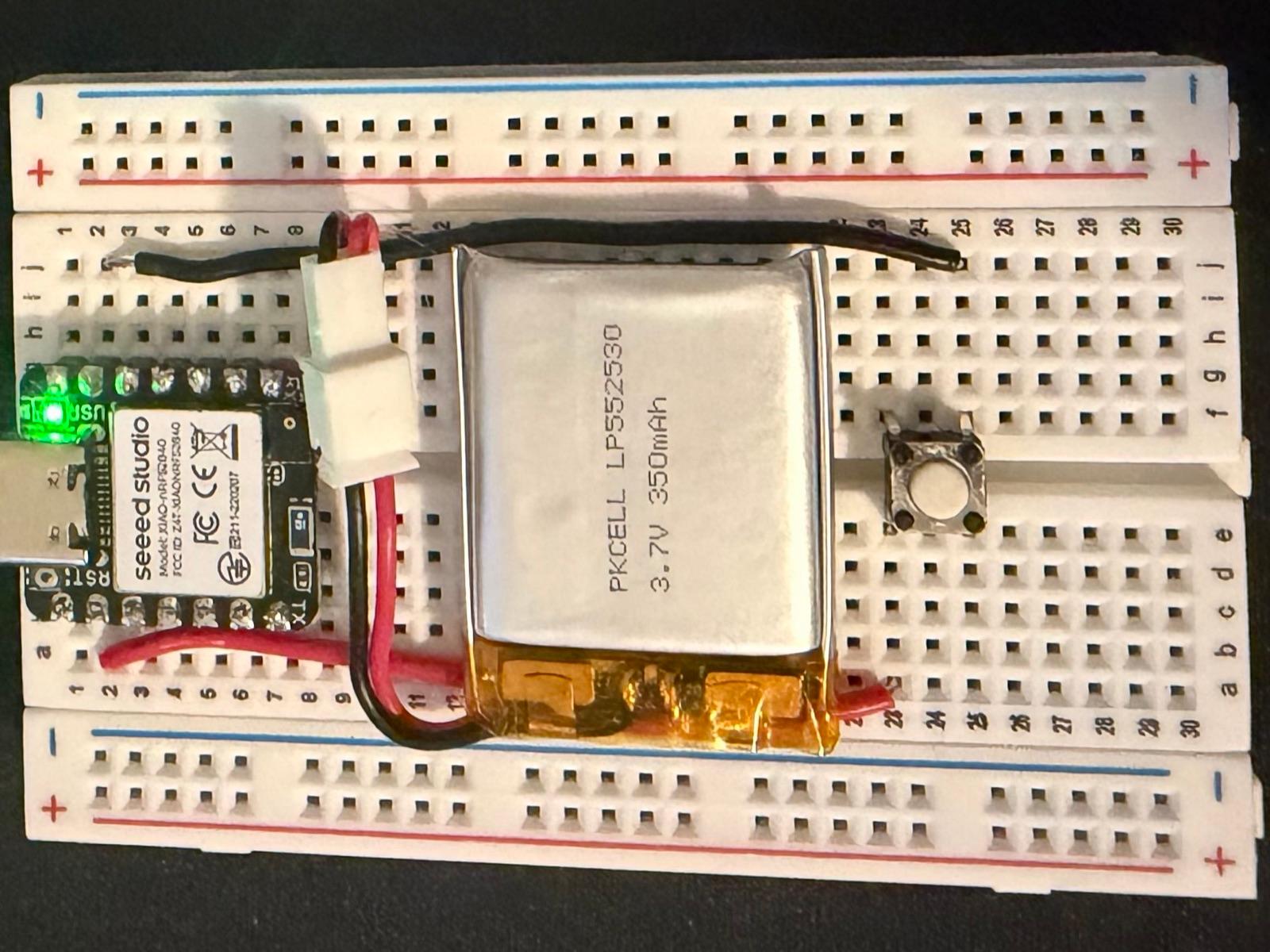
    • Prototype One: XIAO nRF52840 Sense, 350 mAh LiPo and a push button on a breadboard.
  15. The iPhone app, before the hardware

    The software half of Jot works end to end using the phone's own microphone. Hold, speak, release, and the words come back sorted. Here's how it's built and what I learned along the way.

    Update, 3 Oct: sorting now runs on Apple's on-device model by default, with Claude as an opt-in. The XIAO in "Next" was replaced by the custom Rev A board.

    I built the iPhone app before the device (screens are in the App tab). It runs the whole loop with the phone's microphone standing in for Jot, so when the BLE link is ready there's an app waiting for it.

    How it works

    1. Capture. Hold the orb and speak. A waveform follows your voice.
    2. Transcribe. Apple's SpeechAnalyzer turns the audio into words on the phone, and shows them live while you talk.
    3. Classify. The transcript goes to Claude Haiku 4.5, which returns JSON with a type (note, task, reminder or event), a title, details, a due time and any repeat.
    4. File. The item is saved with SwiftData and lands on the Today timeline. Reminders become local notifications.

    What I learned

    • Put the seam in early. The pipeline only sees an AudioSource: a stream of audio chunks. The mic is one implementation and BLE will be another.
    • Tell the model what time it is. "Thursday at two" only resolves if the request includes the current date, time and time zone.
    • Fail toward keeping the words. If classification fails, the transcript is saved as a note anyway.
    • Respect platform limits. iOS allows 64 pending notifications per app, so reminders are scheduled soonest first and rebuilt whenever anything changes.
    • Build the demo in. Debug launch flags load a sample day and script a fake recording, so I could design every screen without a mic or an API key.

    Next

    Swap the mic for the XIAO over Bluetooth Low Energy: M2 on the plan.

  16. Where Jot stands

    Starting the build log. What Jot is, the parts it's built from, and the milestones between here and a first complete unit.

    Update, 3 Oct: the plan below changed. Rev A is a custom board built around a Raytac nRF52840 module instead of the XIAO. The breadboard prototype is still planned: it's waiting on parts. See the Hardware section.

    Jot is a handheld push-to-talk voice-note device. Press the button, speak, release. The recording goes over Bluetooth Low Energy to an iPhone app, which transcribes it and turns it into a note, a reminder, or a calendar event.

    The parts

    • Brain: Seeed XIAO nRF52840 Sense, handling the button, audio capture, and the BLE link.
    • Host: an iPhone app that receives the audio and does the transcription and sorting.
    • Board: a custom PCB, fabricated by JLCPCB.
    • Case: 3D printed.

    The plan to V1

    1. Breadboard prototype
    2. BLE audio to iPhone
    3. Voice to notes, reminders, and calendar events
    4. Custom PCB and 3D-printed case

    The next goal is a first complete unit. Future entries will cover each step as it happens: what worked, what didn't, and why.